Philips Semiconductors
Product data
74F841/74F842
10-bit bus interface latches, non-inverting/inverting
(3-State)
2
2004 Jan 23
FEATURES
∑
High speed parallel latches
∑
Extra data width for wide address/data paths or buses carrying
parity
∑
High impedance NPN base input structure minimizes bus loading
∑
I
IL
is 20
µ
A for minimum bus loading
∑
Buffered control inputs to reduce AC effects
∑
Ideal where high speed, light loading, or increased fan-in are
required as with MOS microprocessors
∑
Positive and negative over-shoots are clamped to ground
∑
3-State outputs glitch free during power-up and power-down
∑
48 mA sink current
∑
Slim dual in-line 300 mil package
∑
Broadside pinout
DESCRIPTION
The 74F841 and 74F842 bus interface latches are designed to
provide extra data width for wider address/data paths of buses
carrying parity.
The 74F841 consists of ten D-type latches with 3-State outputs.
The flip-flops appear transparent to the data when Latch Enable
(LE) is HIGH. This allows asynchronous operation, as the output
transition follows the data in transition. On the LE HIGH-to-LOW
transition, the data that meets the set-up and hold time is latched.
Data appears on the bus when the Output Enable (OE) is LOW.
When OE is HIGH the output is in the high-impedance state.
The 74F842 is the inverted output version of the 74F841.
TYPE
TYPICAL
PROPAGATION
DELAY
TYPICAL
SUPPLY CURRENT
(TOTAL)
74F841, 74F842
5.5 ns
60 mA
ORDERING INFORMATION
COMMERCIAL RANGE: V
CC
= 5 V
±
10%; T
amb
= 0
∞
C to +70
∞
C
Type number
Package
Name
Description
Version
N74F841N, N74F842N
DIP24
plastic dual in-line package; 24 leads (300 mil)
SOT222-1
N74F841D, N74F842D
SO24
plastic small outline package; 24 leads; body width 7.5 mm
SOT137-1
INPUT AND OUTPUT LOADING AND FAN-OUT TABLE
PINS
DESCRIPTION
74F(U.L.)
HIGH/LOW
LOAD VALUE
HIGH/LOW
Dn
Data inputs
1.0/0.033
20
µ
A / 20
µ
A
LE
Latch Enable input
1.0/0.033
20
µ
A / 20
µ
A
OE
Output Enable input (active-LOW)
1.0/0.033
20
µ
A / 20
µ
A
Qn
Data outputs
1200/80
24 mA / 48 mA
Qn
Data outputs
1200/80
24 mA / 48 mA
NOTE: One (1.0) FAST Unit Load is defined as: 20
µ
A in the HIGH state and 0.6 mA in the LOW state.

Philips Semiconductors
Product data
74F841/74F842
10-bit bus interface latches, non-inverting/inverting
(3-State)
2004 Jan 23
3
PIN CONFIGURATION for 74F841
1
2
3
4
5
6
7
8
9
10
11
12
13
14
15
16
17
18
19
20
21
22
23
24
OE
D0
D1
D2
D3
D4
D5
D6
D7
D8
D9
V
CC
Q0
Q1
Q2
Q3
Q4
Q5
Q7
Q6
Q8
Q9
LE
GND
SF01279
LOGIC SYMBOL for 74F841
13
2
SF01280
3
4
5
6
7
8
9
10
1
D0
LE
D1
D2
D3
D4
D5
D6
D7
D8
OE
V
CC
= Pin 24
GND = Pin 12
11
D9
23
22
21
20
19
18
17
16
15
14
Q0
Q1
Q2
Q3
Q4
Q5
Q6
Q7
Q8
Q9
LOGIC SYMBOL (IEEE/IEC) for 74F841
1
15
18
19
20
21
23
2
1 D
SF01281
16
17
5
6
7
8
9
10
4
13
EN
C1
22
3
14
11
PIN CONFIGURATION for 74F842
1
2
3
4
5
6
7
8
9
10
11
12
13
14
15
16
17
18
19
20
21
22
23
24
OE
D0
D1
D2
D3
D4
D5
D6
D7
D8
D9
V
CC
Q0
Q1
Q2
Q3
Q4
Q5
Q7
Q6
Q8
Q9
LE
GND
SF01282
LOGIC SYMBOL for 74F842
13
2
SF01283
3
4
5
6
7
8
9
10
1
D0
LE
D1
D2
D3
D4
D5
D6
D7
D8
OE
V
CC
= Pin 24
GND = Pin 12
11
D9
23
22
21
20
19
18
17
16
15
14
Q0
Q1
Q2
Q3
Q4
Q5
Q6
Q7
Q8
Q9
LOGIC SYMBOL (IEEE/IEC) for 74F842
1
15
18
19
20
21
23
2
1 D
SF01284
16
17
5
6
7
8
9
10
4
13
EN
C1
22
3
14
11
Philips Semiconductors
Product data
74F841/74F842
10-bit bus interface latches, non-inverting/inverting
(3-State)
2004 Jan 23
4
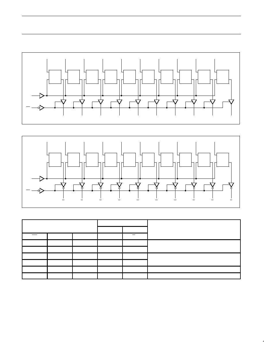
LOGIC DIAGRAM for 74F841
1
OE
V
CC
= Pin 24
GND = Pin 12
L
Q
D
Q0
23
13
LE
D0
2
L
Q
D
Q1
22
D1
3
L
Q
D
Q2
21
D2
4
L
Q
D
Q3
20
D3
5
L
Q
D
Q4
19
D4
6
L
Q
D
Q5
18
D5
7
L
Q
C
D
Q6
17
D6
8
L
Q
D
Q7
16
D7
9
L
Q
D
Q8
15
D8
10
L
Q
D
Q9
14
D9
11
SF01297
74F841
LOGIC DIAGRAM for 74F842
1
OE
V
CC
= Pin 24
GND = Pin 12
L
Q
D
Q0
23
13
LE
D0
2
L
Q
D
Q1
22
D1
3
L
Q
D
Q2
21
D2
4
L
Q
D
Q3
20
D3
5
L
Q
D
Q4
19
D4
6
L
Q
D
Q5
18
D5
7
L
Q
C
D
Q6
17
D6
8
L
Q
D
Q7
16
D7
9
L
Q
D
Q8
15
D8
10
L
Q
D
Q9
14
D9
11
SF01298
74F842
FUNCTION TABLE for 74F841 and 74F842
INPUTS
OUTPUTS
INPUTS
74F841
74F842
OPERATING MODE
OE
LE
Dn
Qn
Qn
L
H
L
L
H
Transparent
L
H
H
H
L
Transparent
L
l
L
H
Latched
L
h
H
L
Latched
H
X
X
Z
Z
High Impedance
L
L
X
NC
NC
Hold
H = HIGH voltage level
L
= LOW voltage level
h
= HIGH state one set-up time before the HIGH-to-LOW LE transition
l
= LOW state one set-up time before the HIGH-to-LOW LE transition
= HIGH-to-LOW transition
X = Don't care
NC= No change
Z = High impedance "off" state
Philips Semiconductors
Product data
74F841/74F842
10-bit bus interface latches, non-inverting/inverting
(3-State)
2004 Jan 23
5
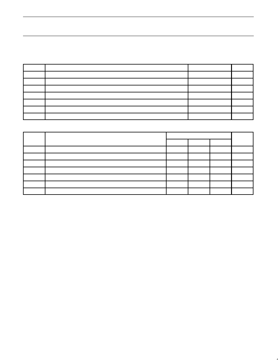
ABSOLUTE MAXIMUM RATINGS
Operation beyond the limits set forth in this table may impair the useful life of the device.
Unless otherwise noted these limits are over the operating free-air temperature range.
SYMBOL
PARAMETER
RATING
UNIT
V
CC
supply voltage
≠0.5 to +7.0
V
V
IN
input voltage
≠0.5 to +7.0
V
I
IN
input current
≠30 to +5
mA
V
OUT
voltage applied to output in HIGH output state
≠0.5 to V
CC
V
I
OUT
current applied to output in LOW output state
84
mA
T
amb
operating free-air temperature range
0 to +70
∞
C
T
stg
storage temperature range
≠65 to +150
∞
C
RECOMMENDED OPERATING CONDITIONS
SYMBOL
PARAMETER
LIMITS
UNIT
SYMBOL
PARAMETER
MIN
NOM
MAX
UNIT
V
CC
supply voltage
4.5
5.0
5.5
V
V
IH
HIGH-level input voltage
2.0
≠
≠
V
V
IL
LOW-level input voltage
≠
≠
0.8
V
I
IK
input clamp current
≠
≠
≠18
mA
I
OH
HIGH-level output current
≠
≠
≠24
mA
I
OL
LOW-level output current
≠
≠
48
mA
T
amb
operating free-air temperature range
0
≠
+70
∞
C